Cascoded JFET Current source
Looking around the internet to find a current source for my Ulti-Preamp which can be built without having to buy a bunch of FETs and pick the best one, I stumbled upon the cascoded FET current source. It is still heavily dependent on the characteristics of the FETs, but since there are now two of them, it might be easier to pick two 'diametrically opposite' parts and get away without matching them. A great article about this subject is Sources 101 by Walt Jung. It covers basically everything you have to know to build one and shows the great performance with nice Audio Precision plots. Since I have a couple different JFETs around, I gave it a shot and show you the results of my testing here.
For this circuit to work well, there's one thing you have to look out for. The voltage Vdg from Drain to Gate over any of the JFETs should be at least two times larger than the Vgsoff of that JFET. For the cascode JFET (the 'upper one', J2) this is easily achieved when you have enough voltage to apply to the whole circuit. Vdg over J1 will be maximised by picking J1 with the lowest possible Vgsoff, and J2 with a higher Idss and also a higher Vgsoff (with -4V being higher than -1V that is). The circuit will still work as a current source even if that condition is not met for J1, but the achievable maximum output current and the transresistance will be limited. I did not test the dynamic performance, so I can't tell if that will be limited, too. Also remember that the upper JFET will see most of the working voltage, so make sure it can handle it.
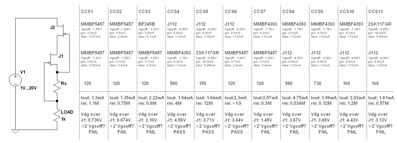
The circuit with all the parts and combinations that I measured
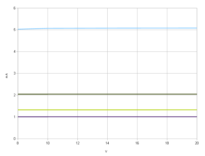
From all the 11 combinations that I built and tested (and they're certainly not all that were possible), only three were able to meet the ''J1 Vdg > 2 * Vgsoff'' goal. They also happen to be the three circuits with the highest transresistance. A high transresistance means that the output current changes only very little in accordance to the working voltage. The best circuit managed to keep the current steady over a voltage range of 12V (which translates to an infinite transresistance), while the worst changed output current by as much as 350uV over the same 12V (~7% of the maximum current in that case)!
The circuits CCS1 and CCS2 were built from a batch of MMBF5457. I randomly picked four parts from the bin and put them on the DCA75 parts tester to measure their characteristics. Then I chose J1 < Vgsoff < J2 for CCS1 and the other two parts with J1 > Vgsoff > J2 (the other way round) for CCS2. Since all of the measured values are pretty close to each other due to the JFETs being from the same batch, I didn't expect much differences between the two circuits. Furthermore I didn't expect to meet the ''J1 Vdg > 2 * Vgsoff'' goal, since I believe that J2 Vgsoff has to be at least double that of J1.
The test results seem to support this. J1 Vdg is about half of Vgsoff instead of two times that, and the transresistance is around 1 Megaohm or a little less, with CCS1 faring slightly better. The output current is a modest 1.3mA for two devices measuring 2.8mA and 3.4mA respectively. Of course the Source resistor with 120R takes some current away here, but it helps with transresistance, as the following tests will show.
The next circuit CCS3 is based on CCS2, with the upper JFET swapped for a BF245B. This one has roughly twice the Vgsoff (-3.22V to -1,49V) and thrice the Idss (9.1mA to 2.9mA) of the MMBF5457 it replaces, with transconductance gm in the same ballpark as J1 and J2 (3.5mS and 3.7mS). That should increase the Vdg for J1 and thus help the circuit to achieve the goal (''J1 Vdg > 2 * Vgsoff'', remember? ;) I'll just call it ''the goal'' from now on).
J1 Vdg actually increased to 2.10V, which is plenty compared to the former 0.674V, but still not enough unfortunately. With a Vgsoff of -1.6V we would have needed at least one Volt more to achieve the goal. The transresistance actually dropped down from 750k to only 600k, but the output current increased to 2.22mA. Due to the output current now exceeding 2mA I had to change the measurement range of my crappy old stationary lab multimeter and thus lost some precision, but the trend is clearly seen. Not looking all too well, so let's try something different for a change.
Next up comes CCS4 with an all new setup. This time we have a beefy J112 with lots of current and a higher transconductance for the upper FET, and a just-as-beefy MMBF4393 for J1, but with a somewhat lower Vgsoff of -1.78V compared to the -4.0V of the J112. More than twice the difference, looking good in theory! To keep the output current in the range of 2mA it was necessary to increase Rs this time. I found a 560R measuring 580R, which put the current just shy of 2mA, almost maxing out the accurracy of the multimeter range; nice.
J1 Vdg measured a whopping 4.56V, which is 2^8/100 times Vgsoff, and thus achieved the goal for the first time! Transresistance is a nice 4M now, much much better than the previous 600k. Output current is miniscule, but deliberately so. We'll increase it later on with another circuit to see the effect of Rs. For now it pretty much looks like lots of open loop gain (high Idss) and lots of negative feedback (high Rs) help to improve the overall circuit – sounds familiar? ;)
On to CCS5. Let's keep the J112 for the cascode FET and toss the MMBF4393. Let's use a part with a really low Vgsoff of only -0.65V now. Please welcome the 2SK117GR, the little brother of everybody's darling, the ubiquitous and unobtainium (well, somewhat; expensive and often faked) 2SK170. Idss is a modest 5.45mA and gm a solid 16.0mS. A good looking combination.
And it's true. J1 Vdg is 3.71V, almost six times Vgsoff: GOAL!! Transresistance increased again to 12M, but it might have just as well been infinite. To calculate rm I used the difference in output current over a working voltage range of 12V, namely from 8V to 20V. If I had taken the values from 10V to 20V this time, the result would have been infinite. So we're dealing with a very good result here indeed! Output current is again a little on the low side with 1.64mA for a 5.45mA device, using only 150R source resistance, but the overall performance is great.
CCS6 keeps the J112 around as the upper JFET for a third time, now in combination with the lower MMBF5457 from CCS2 and CCS3. So now we have a high-current, high-gain, high-Vgsoff device cascoding a low-current, low-gain and moderately low Vgsoff device.
This time the transresistance actually calculates to infinity. J1 Vdg is 3.61V and the goal is easily met. Output current is a steady 2.3mA (from a 3.4mA device). In fact, this is the best performing circuit of them all, but I'm not sure why!
Let's compare it with the previous two, which use exactly the same cascode FET. Here we have a Vgsoff of -1.6V, lying in between the -0.65V and -1.78V of the other two, but still being the best. That probably can't be it. Transconductance is the lowest of the three, as is the drain current Idss. Maybe one of those it is, or even the combination of them both being as low as possible? I'll have to investigate that further.
Let's do another variation on the theme. For CCS7 we keep the humble MMBF5457 in the lower place and this time stack the MMBF4393 on top, which used to be the lower one in CCS4. The MMBF4393 measures rather similar to the previous J112, with just a tad more gm, high Idss, but just about half the Vgsoff with -1.78V. Now we have a situation similar to CCS1, with Vgsoff of J1 and J2 being almost equal, but with gm and Idss of J2 being much higher, like in the previous circuit CCS6.
J1 Vdg dropped down to a measly 1.45V, which is actually lower than Vgsoff! No goal this time. Transresistance also dropped to only 300k, the worst result so far. Output current dropped only a little, from 2.3mA to 2.07mA, but the overall performance doesn't look all too well. But hang on, we can do worse...
Introducing CCS8, 9, and 10, we again keep the upper MMBF4393 and replace the lower part. This time for the tried-and-tested J112, used for the first time in the position of J1. Now we have two parts with high gain and high current, but with a twist in Vgsoff. The lower Vgsoff part belongs to position J1, like we did in CCS4, or does it? Honestly I didn't expect this circuit to perform any good, but I tested it anyway. Since the J112 is a high current part, I started out with the higher Rs from CCS4.
Contrary to CCS4's rather modest 1.94mA I now got a whopping 4.75mA output current! Still not a lot for a >12mA part, but certainly more than I had expected. The reading of >12mA for both parts seems to be a little indefinite here. J1 Vdg measures only 3.67V, lower than the -4Vgsoff, which was to be expected. Likewise the transresistance is down to an all-time-low of only 34k! It's actually not that bad when you grant this circuit three or four more volts, but it's still nothing to rave about then.
So much for CCS8. CCS9 is the same circuit, except for an added 120R source resistance, for a total of 730R. This brings down the output current a little, from 4.75mA to 3.96mA. J1 Vdg increased a little from 3.67V to 3.88V, as did the transresistance.
CCS10 again just increased the source resistance, to 1k6 this time, for an output current of 2.02mA. J1 Vdg raised a little to 4.43V, but is still far from the goal. Transresistance is a considerable 1.2M now, about as bad as the first one or two circuits I tested. Certainly worse than CCS4, which uses the exact same two JFETs and yields about the same output current.
Just for the fun of it, here's CCS11, keeping the J112 on the lower side and putting the low-Vgsoff 2SK117GR on top. It's CCS5 with swapped transistors, like CCS4 and CCS10. The results are basically the same: J1 Vdg lower than Vgsoff and a transresistance around half a megohm. No great performer and probably to be avoided in the real world.
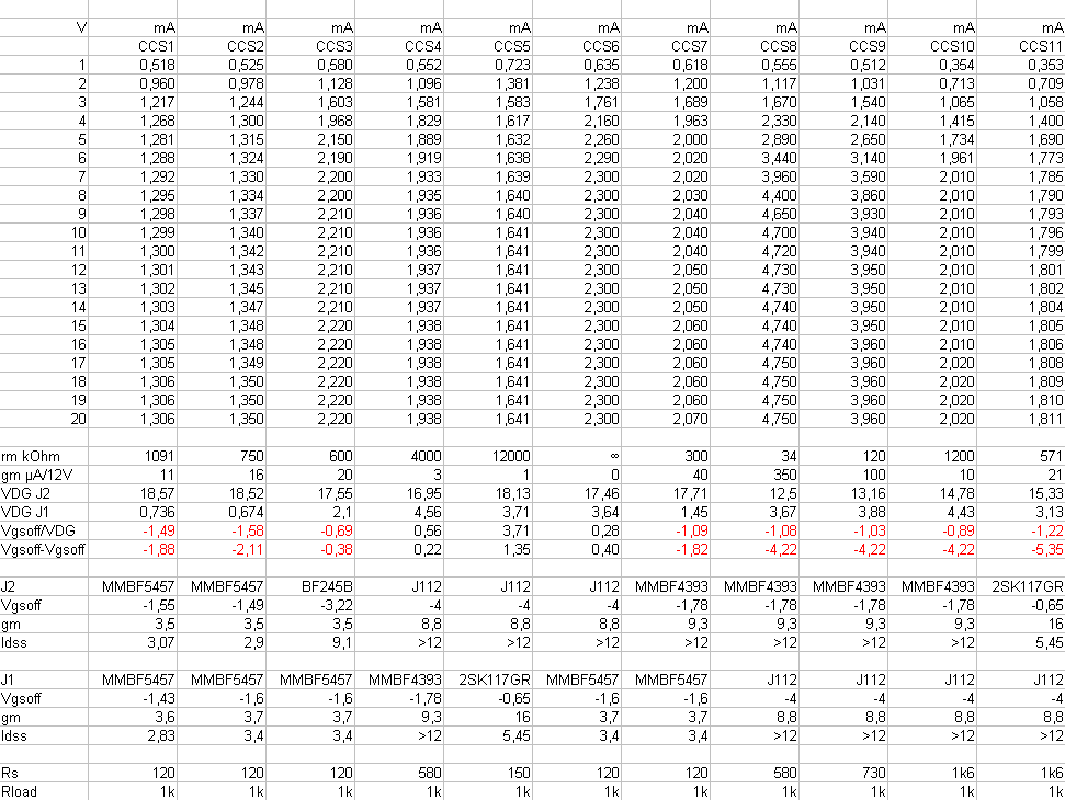
All the collected data in one go

...and something a little colorful :)
06.10.2018
I have made some more measurements today. Let's start out with CCS4, which was a good performer in the first measurement run. I used the same circuit, but swapped the source resistor Rs for a 500R trimpot. To save myself some time I only tested four voltages this time, namely 8V – 10V – 15V – 20V, and noticed afterwards, when I had made all the measurements, that I didn't measure J1 Vdg. Bummer, but it'll have to do without for now. The trimmer was set to the measured values of 0.7R – 100R – 200R – 300R – 567R.
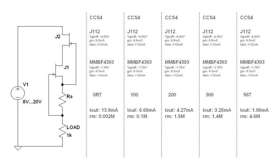

One thing you can tell at a glance is: the higher Rs, the better the performance. Of course you could argue that the circuit with a low or no Rs simply needs more voltage to reach into the linear region, but what's the point in that if the upper JFET is already close to its maximum voltage? We're still save here with 20V for a 35V part, but that's a huge caveat for the higher current version. The 300R variant at 10V is just as good as at 20V and very probably at 30V too, while the 0.7R variant is not. One conclusion to draw from this case would be that the cascoded JFET current source is a great performer with output current being at least two times smaller than J1 Idss, as long as J1 Vgsoff is two times smaller than J2 Vgsoff, too. I'd need some more JFETs to prove that...
I also tested CCS5 again, which was a stellar performer and my hope for an easy to pick solution. The 2SK117GR is specced with a Vgsoff in the range of -0.2V to -1.5V, while the J112 ranges from -1V to -5V. That looks like it would be pretty easy to pick any of them and get away with a working circuit. I'd love to test a 2SK117 with -1.5V and a J112 with only -1.0V as cascode JFET – unfortunately I don't have two such parts :( .
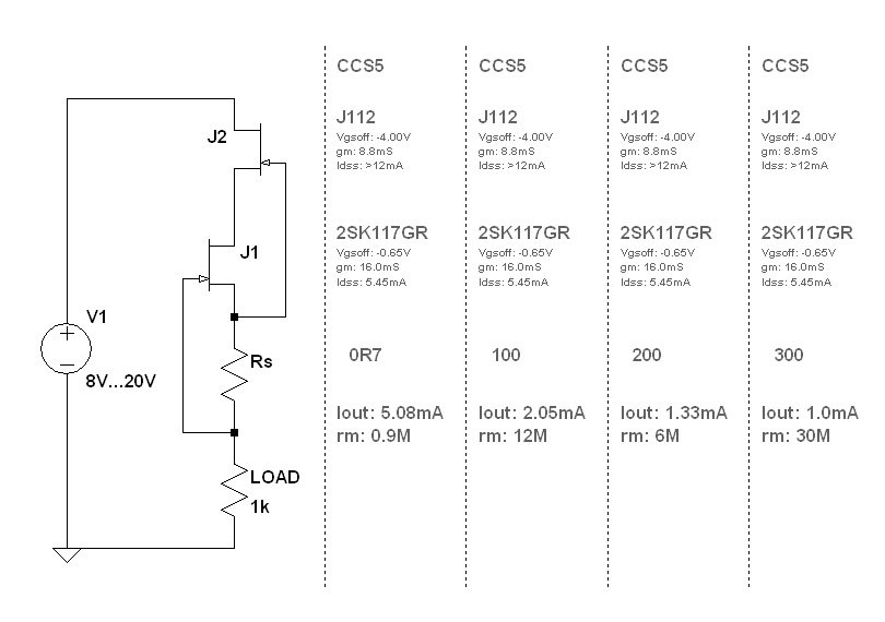
And again the performance is exemplary. Even without any source resistance the circuit works great from 10V on, yielding over 90% of J1's Idss. Like I said I didn't measure J1 Vdg here, but I guess that it's still above 2 * Vgsoff.
Finally I tested the circuit with two J112, quite like the first CCS1 with two equal MMBF's. And to have something to compare to, I also tested a single J112 with a source resistance of 1k6, without the cascoding J2.


As you can see at a glance from the graph, this circuit is practically unusable. It behaves more like a simple resistor than a current source. Conclusion to remember: a single J112 as current source is better than two cascoded ones!
Here's one more graph that I created as a comparison. Since I am looking for a current source yielding 2mA, I plotted the according circuits together with the single JFET variant.
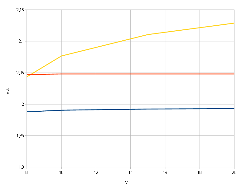
The yellow graph shows the single J112 with a 1k6 source resistor. The blue graph shows the same J112 cascoding a MMBF4393 with 567R source resistance, and a dramatic improvement. The almost straight red line again shows the same J112, cascoding a 2SK117GR with 100R source resistance this time, for an even better improvement.
To conclude I would state the following: Done right and picking the right parts the cascoded JFET current source is a stellar performer, but without spending some time on matching the parts or even picking two of the same kind, the performance will be worse than a simple resistor!
10.10.2018
Being not totally satisfied with the criteria to pick the right JFETs, I've investigated the measurement data of my devices a little closer.
The best pick for the cascode FET J2 seems to be the cheap and readily available J112. With an Id >10mA it is a good allrounder for output currents <10mA and Vgsoff seems to be in a favorable range (-1V...-5V). The J111 has even more Id, but together with a usually higher Vgsoff (-3V...-10V) the final current source would need a lot more working voltage to achieve best performance. A transconductance >5 seems to be favorable, too.
Now how to pick J1? First of all, the lowest possible Vgsoff is one thing to look out for. Unfortunately a low Vgsoff also brings a low Id, which is important for higher output currents >5mA or so. One way to compensate for a low Id is to put two or more JFETs in parallel. I have tested this with two MMBF5457 soldered on top of each other, and they seem to work just fine. The pinchoff voltage of the compound device will be that of the device with the highest Vgsoff (in my case -1.6V, from -1.49V and -1.6V), while Id and gm will roughly add up. But a low Vgsoff alone doesn't seem to be the only thing, so my first thought was that a higher transconductance will be better. The good results with a single MMBF5457 seem to contradict that, though. The 2SK117 with the lowest Vgsoff of -0.64V has a rather high gm of 16.1mS, but is not necessarily better than the MMBF5457 with a worse Vgsoff of -1.6V and a much worse gm of only 4.2mS. On the other hand, the MMBF4349 with a Vgsoff close to that of the MMBF5457 (-1.78V) has a somewhat higher gm with 9,3mS, but doesn't perform any better!
There's one more value that the DCA75 spit out, namely Vgson. I didn't pay any attention to this value before, since I couldn't find something remotely like it in any of the datasheets for my devices. It's probably a little over my head; I'm still no FET guru after all ;) .
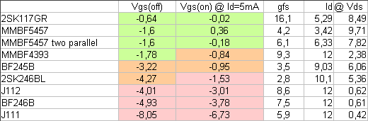
I've put all that DCA data in a little table and tried to sort it for 'best pick for J1' from top to bottom. The values that seemed most important to me got some coloration, according to my measurement results so far. As you can see, the best contenders all have a Vgson which is within a volt around 0V, or even a little higher. The 2SK117 and MMBF5457 fare pretty well here, whereas the MMBF4393 has a noticeably higher Vgson. That might explain why it doesn't perform any better than the other two. The next part has a pretty high Vgsoff already, together with a highish Vgson, and it is indeed a weak performer.
So, this might be the two parameters to cherry-pick: Vgsoff and Vgson. The first one is easily spotted from the datasheets, but where to get the other one from, if not from a measurement? Any ideas; please let me know!