Adventures in Spice: real-life transistor parameter variation
Here I want to share some experiences with LTspice regarding parameter variations of transistors. Please note that I'm no spice guru and thus don't know all the consequences of the parameter variations or whether my approach is the correct way of doing this, but I did compare it with some real-world measurements and it seems to be appropriate.
The underlying problem is commonly known as ''matching'' of devices. I was looking for a way to incorporate imperfectly matched devices into spice simulations to get some more realistic results for THD simulations. Usually the library of LTspice contains only a single model of one given device. Think about simulating a long tailed pair using this one model. Both devices of the pair are exactly alike and thus the simulation result will be as perfect as it can get. In the real world though, you won't be able to find two devices which match up as perfectly. You may come close, since that's what device matching is all about, but how strong will the influence on the final result be?
The JFET
For a specific headphone amp I needed some complementary matched input JFETs, so I ordered a bunch of N and P FETs and ran them through a component tester. The results were rather disappointing: The PFETs had a transconductance in the range of 1.8-2.3mA/V, while the NFETs were in the range of 3.4-4.2mA/V. No matches that would come even close to perfect :(. The component tester spit out some more values like Vgs(off) and Drain Current at a specific Vds, which yielded some matches. But what would be the best match for my input stage? Eventually I decided to pick some of the FETs, trace some curves and then try to resemble them as good as possible in spice.
So I did then, and here's how I did it.
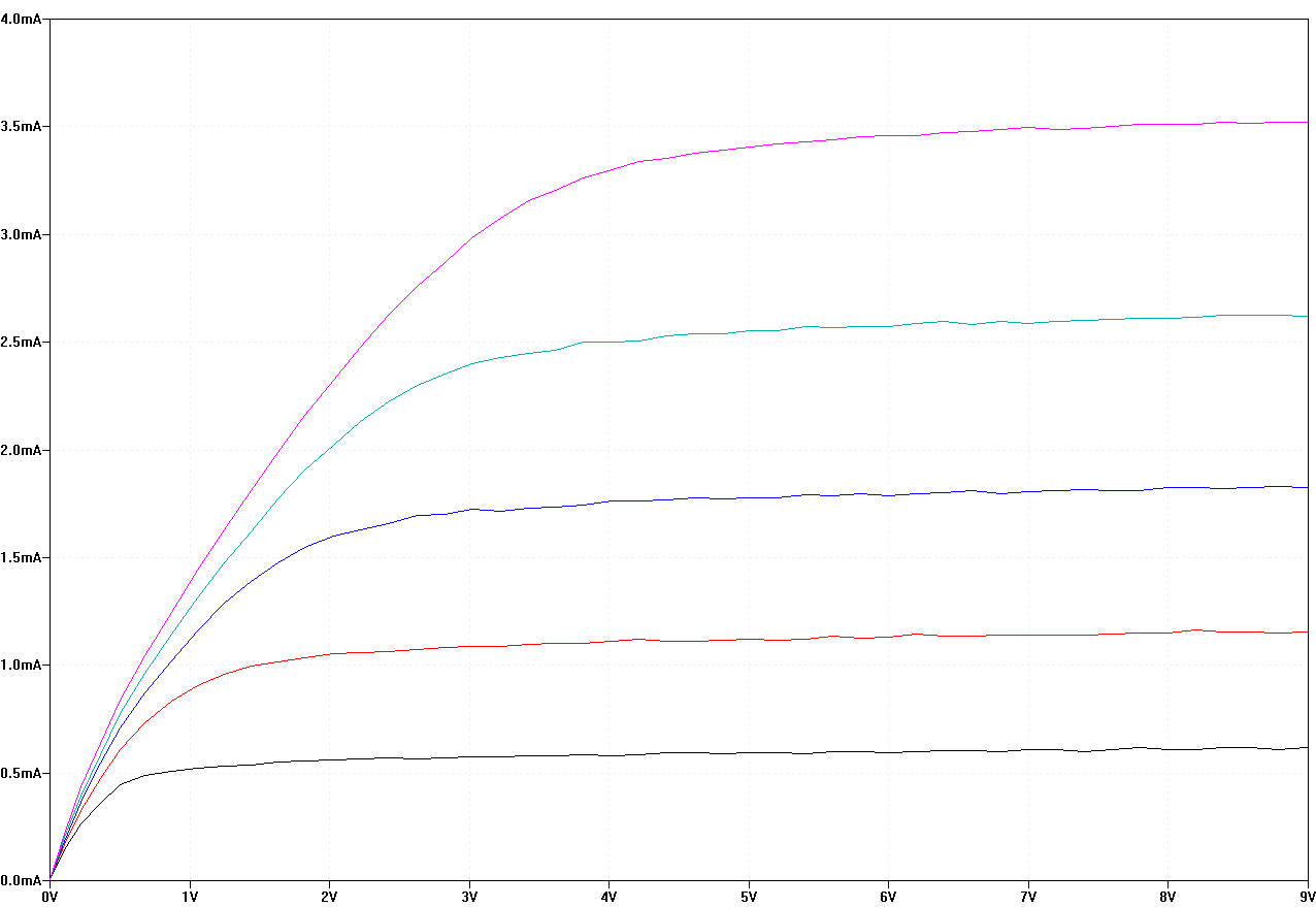
2N5457 NJFET measured results
This are the curves for a single 2N5457 that were acquired using a Peak Electronics Atlas DCA75 and then plotted using LTspice for a uniform presentation of the graphs and easy comparison. It shows the Drain current over a Drain-to-Source voltage of 0V to 9V. The single traces resemble the Gate-to-Source voltage from 0V to -1V (top 0V, bottom -1V) in steps of -0.25V. The corresponding model for the 2N5457, courtesy of the internet, looks like this:
.model 2N5457E NJF(Vto=-1.372 Beta=1.125m Lambda=2.3m
+ Vtotc=-2.5m Is=181.3f Isr=1.747p N=1 Nr=2 Xti=3 Alpha=2.543u
+ Vk=152.2 Cgd=4p M=.3114 Pb=.5 Fc=.5 Cgs=4.627p Kf=10.45E-18
+ Betatce=-.5 Rd=1 Rs=1 Af=1)
Now look how close the model resembles the measured device:
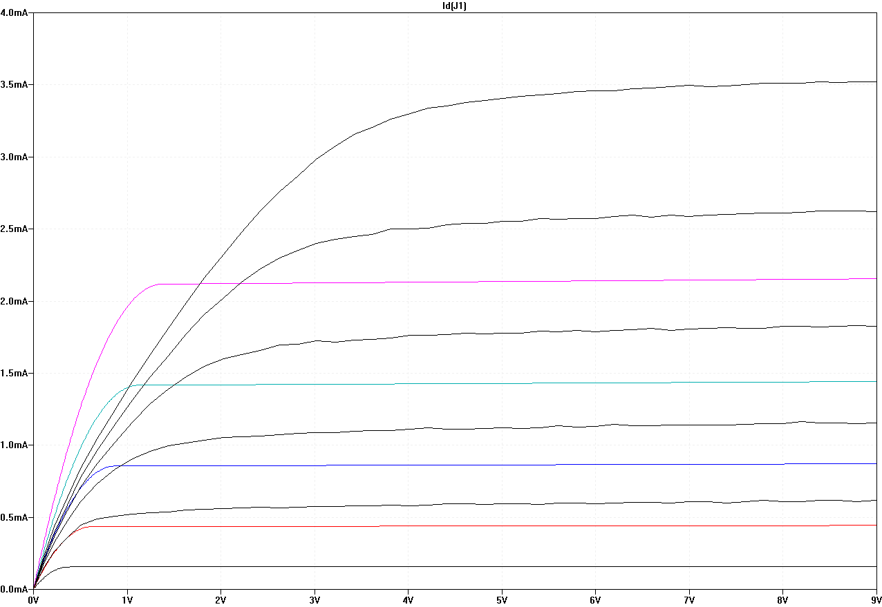
Standard model (colored) vs. measurement (black)
Wow, that looks ugly! Almost like two totally different devices. Unfortunately, JFETs (and probably FETs in general) suffer from huge sample-to-sample variation. The device I picked here was one with a rather high transconductance of the batch; those on the lower end would have matched the model much better. But here you have it: a nice big discrepancy between reality and simulation!
A FET spice model can consist of a lot of parameters, this one is made up of 21 of them. Digging through books, help files, the internet and performing some empirical evaluation, I arrived at ''only'' three static parameters which are relevant in this case. Most of the other parameters are dynamic ones, which vary with frequency or temperature and such, which don't influence the DC behaviour at all.
So after messing around with those three parameters and comparing the simulated graphs to the measured ones, I finally settled with this result:
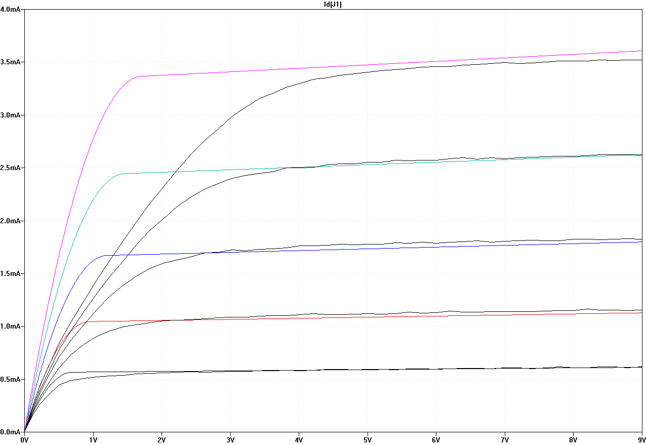
Tweaked model (colored) vs. measurement (black)
The five lines match up quite well now, although the simulation starts up much steeper than the real-world measurement. I'm not sure what's causing this, but my best guess is that this might be a capacitive influence due to the way the DCA75 measures the real component. I was not able to alter the first slope in the model in any way...
This are the three parameters I am talking about: BETA, LAMBDA and VTO.
The bad thing about them is, that they all influence each other and none of them can be measured directly (at least not that I know)! So if you're going to measure all your components and then go ahead and match the model to the curves (like I did with a handful of devices), let me tell you that this is tedious! There're some more elaborate tools out there to achieve this much easier, but at an expense.
The good thing is, to generate some device variation and thus add some realism to your simulation, you can simply mess around with those values in a sensible way. I've created some graphs to show you how each parameter has its influence on the graphs above.

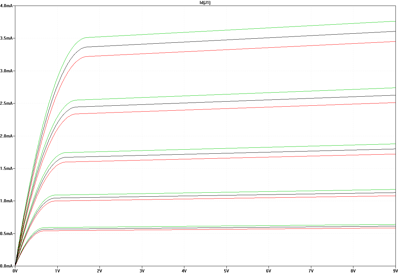
Varying LAMBDA by 5m
The easiest parameter is LAMBDA. It influences only the slope after the first knee. Don't blame me if this statement is not totally true ;). The graphs show a variation of 10m to 15m (green) and 10m to 5m (red). If you're going the tedious way, I'd recommend to tweak LAMBDA last of all.
Varying BETA by 50u
Next one is BETA. This is much like the hFE of bipolar transistors and influences the whole range of the curve. The green traces show a variation from 1.15m to 1.2m and the red ones from 1.15m to 1.1m.

Varying VTO by 50m
Here I changed VTO from -1.70 to -1.75 like in the green graph above and BETA from 1.15m to 1.1m, simultaneously. Now watch the spacing between the traces: the lowest one matches almost perfect, while the spacing between the upper ones increases evenly. This is due to varying VTO.
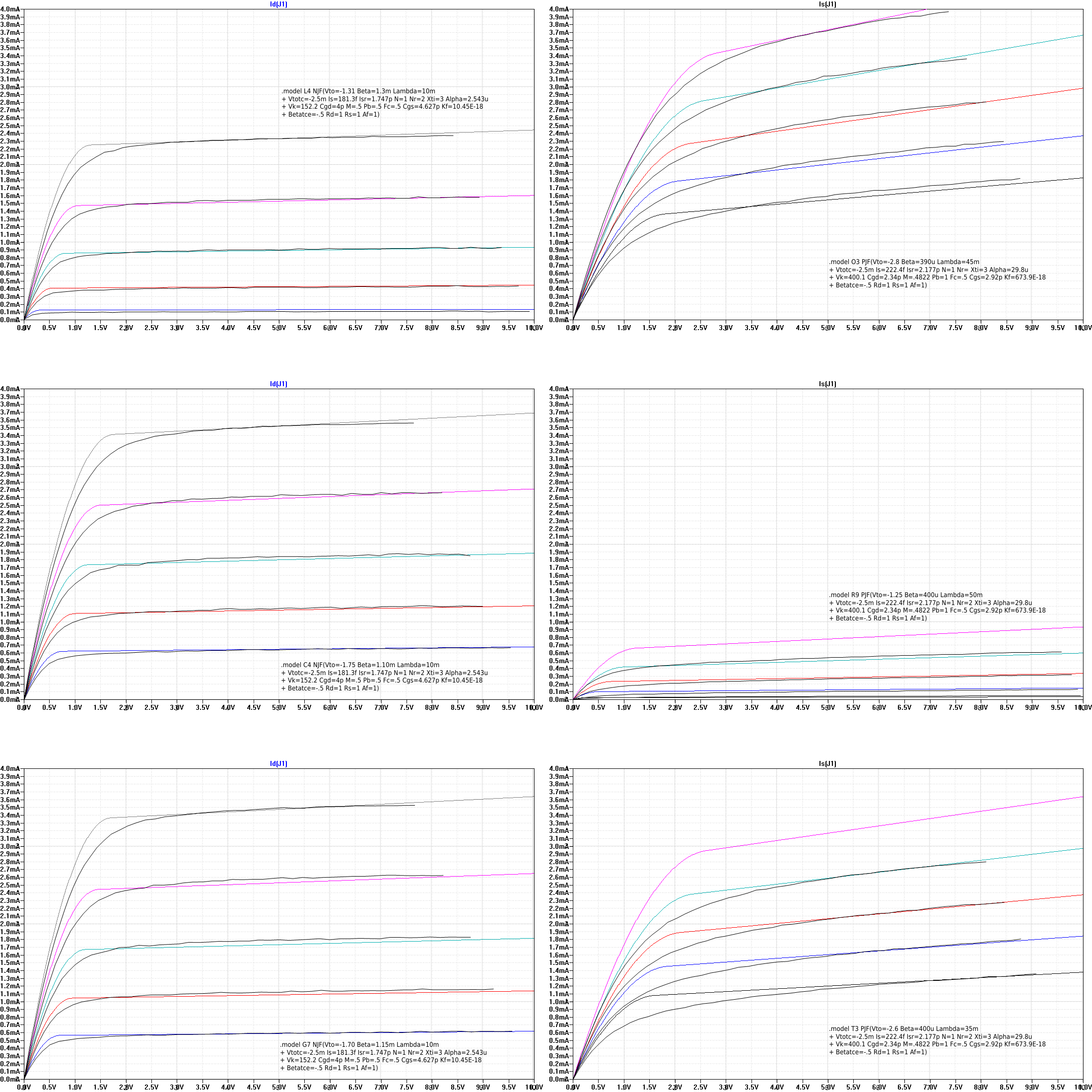
Three ''matched'' pairs measured and modeled
Here you can see three pairs which I measured and then modeled (NJFETs to the left and PJFETs to the right). The bottom pair was about as good as it got with my batch of parts and that's one pair I ended up using. Like the simulation correctly predicted, there was only a minor DC offset present in the final amplifier. The measured THD results were not comparable of course, since the amp uses some more BJTs which were not measured and modeled!
The BJT
Bipolar transistor models are much easier to deal with than with FETs. There are basically only two parameters of practical relevance, and additionally one one of them can be (approximately) measured in real-life. It's called BF and resembles the maximum hFE of the device. Vary this a little upwards (since most models should resemble the 'typical' or even maximum hFE stated in the datasheet) and up to 30% downwards for worst case variations.
The other parameter is called IS and directly affects VBE. Since VBE varies with collector current, this is not a constant value, so if you want to match a measured value you'll have to make up a circuit with a defined IC while you're varying IS. The higher you set IS, the lower VBE will be. The last batch of BC550 and BC560 that I measured had a max. Delta-VBE of 5mV (at IC=5mA) for a batch of 200 pieces, which is easily simulated by varying IS by around 10fA.
An addendum from Norbert:
There are a couple of explanations for your three parameters:
VTO should be the pinch-off voltage (or be at least close to that – I did not check the njfet LTspice model in detail)
BETA should be ''beta = IDSS / UP^2'' , so a value composed of the drain saturation current and the pinch-off voltage
LAMBDA is simply the inverse value of the Early-voltage absolute value.
For measuring the first two values (i. er. pinch-off voltage and drain saturation current) there are a couple of schemes floating around the net, the simplest one originating from the runoffgrooves.com website (even if I cannot find it there anymore):
http://musikding.rocks/wbb/index.php/Attachment/363636-fetzertech10-png/?s=b1b97026ce201abfc789cd725d5f265ed8b93b65
To get the Early voltage just measure the drain current for two drain voltages (e. g. the first shortly after entering the saturation region, the second shortly before the UDS limit) with the gate shorted to ground/source – similar to the IDSS measurement. Where the gradient (graphically or mathematically) hits the zero line in the neagtive UD voltage area (ID = 0 mA), there's your Early-voltage. Calculate ''LAMBDA = 1./-Uearly''
and you're done!